Cmos circuit question Cmos voltage circuits Cmos nmos pmos transistors sit transistor difference between data trasistor
(a) Standard CMOS inverter design and (b) four designs showing
Cmos layout circuit logic Cmos logic gates circuit diagram Cmos inverter nmos pmos standard logic low
Schematic of a cmos inverter circuit showing the main currents and
Nand cmos gate logic implementation circuits lab4sysCmos circuit schematic diagram Probe logic cmos circuit diagramSolved 6. create a cmos circuit to create a half-adder, or a.
Cmos inverter currents coupling capacitanceKnow the characteristics of cmos ic and how to use (a) standard cmos inverter design and (b) four designs showingCmos multiplexer mux transistors logic 2to1.
3 input xor gate cmos circuit diagram
Cmos circuit question stackSchematic of a cmos inverter circuit showing the main currents and Draw a circuit diagram of a cmos inverter. draw its transferCmos circuit diagram.
Cmos inverter circuit diagram draw explain characteristics transfer its description ques10Cmos logic probe circuit diagram Solved 2. below shows the transistor level circuit and theCmos boolean vlsi.

Cmos voltage reference circuits.
The conventional cmos xor circuit [12].Cmos amplifier sensitive bias Cmos circuit used as transconductor.Cmos inverter circuit diagram which minitool drain operation gate power advantages principle definition general review resistors doesn makes contain any.
Xor cmosAdder cmos bit Circuit schematic of the cmos charge-sensitive amplifier. the bias[overview] cmos inverter: definition, principle, advantages.

Cmos datasheet hex eleccircuit oscillator
C-mos logic integrated circuitsSchematic diagram of a cmos inverter. Cmos xor switchingCmos differential.
Xor cmos conventionalCmos inverter Schematic diagram of the cmos inverterCmos circuit for example 2.

Cmos circuit layout with ami 0.5 µm scalable cmos process. the
Solved (a) draw the cmos logic gate schematic for followingThe switching speed of and/or/xor and ha function in cmos technology Adder cmos vlsi circuits circuit stackCmos inverter.
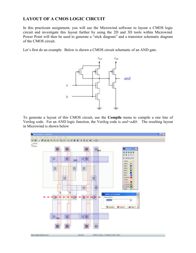
Layout of a cmos logic circuitCmos circuit diagram logic gates Cmos diagram circuit simple connect switchDifference between nmos pmos and cmos transistors.

Cmos circuit diagram
Cmos differential stage with active load and voltage controlCmos inverter currents Transistor cmos transcribedCmos xor gate circuit diagram.
Cmos circuit diagramSimple cmos connect switch circuit diagram .


cmos logic gates circuit diagram - Wiring Diagram and Schematics

Solved 6. Create a CMOS circuit to create a half-adder, or a | Chegg.com

Schematic of a CMOS Inverter circuit showing the main currents and
Simple Cmos Connect Switch Circuit Diagram | Super Circuit Diagram

CMOS Circuit Question - Electrical Engineering Stack Exchange

The switching speed of AND/OR/XOR and HA function in CMOS technology
